
熔融石英概述
定义和生产
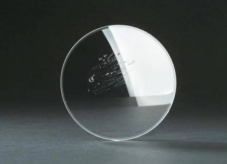
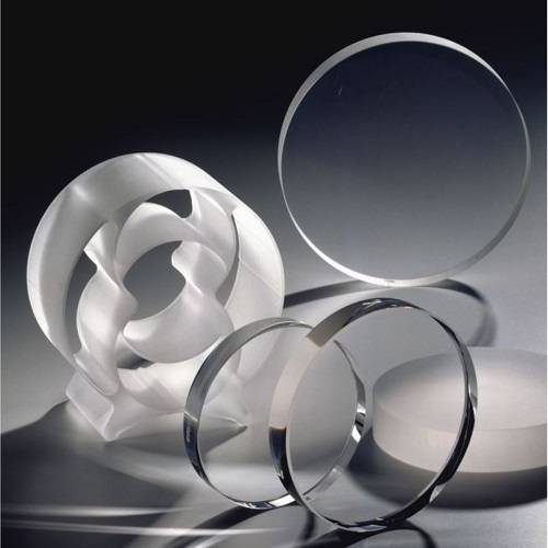
熔融石英是一种无定形的氧化硅,通过在高温下控制优质硅原料的熔化而精心制作而成。这一过程通常在专用熔炉中进行,可确保去除杂质,形成高纯度的玻璃状物质。熔融石英的生产是获得各种高科技产业(包括半导体制造、光伏、航空航天和光纤通信系统)所需材料的关键步骤。
根据具体的质量和应用要求,这种转变所需的高温通常在 1700°C 至 2000°C 之间。这些极端条件有利于二氧化硅颗粒的均匀熔化,从而形成均匀、透明的玻璃。熔融石英具有高纯度、热稳定性和低热膨胀性等优异性能,是要求精确度和可靠性的应用领域的理想材料。
生产过程不仅要实现高纯度,还要保持材料性能的一致性。从原材料的选择到熔融石英的最终冷却和成型,每个阶段都需要采取严格的质量控制措施。熔融石英行业的公司不断投资于先进技术和设备升级,以提高生产过程的效率和精度,确保最终产品符合客户的严格要求。
总之,熔融石英的生产是一个复杂而重要的过程,是许多技术进步的基础。通过精心控制熔化和冷却过程,生产商可以生产出高纯度和热稳定性的材料,使其成为各种高科技应用中不可或缺的材料。
特性与应用
熔融石英以其高纯度和优异的热稳定性而闻名,在各行各业都有广泛的应用。在半导体领域,它是光刻工艺中的关键材料,可确保在晶片上形成精确的图案。这对制造复杂的半导体器件至关重要。
在光伏行业,熔融石英是制造太阳能电池不可或缺的材料。它的高透明度和热阻特性使其成为光学元件和衬底材料的理想材料。这有助于提高光伏系统的效率和使用寿命。
航空航天工业也受益于熔融石英的独特特性。熔融石英的热冲击稳定性使其成为飞机结构部件的绝佳选择,因为飞机结构部件对极端温度变化的抵抗能力至关重要。这确保了航空结构的耐用性和安全性。
此外,熔融石英还可用于通信系统的光纤制造。熔融石英具有低光衰减和高抗拉强度的特点,可以在长距离传输数据时将损耗降到最低。这一应用凸显了熔融石英在现代通信网络中的重要性。
总之,熔融石英的各种特性使其在半导体制造、光伏、航空航天和通信系统中不可或缺,推动了这些关键领域的技术进步并提高了性能。
技术创新
半导体和光伏领域
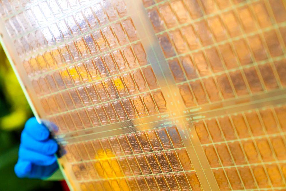
半导体和光伏领域的创新主要是为了提高熔融石英在两个关键领域的性能:光刻技术和光伏电池制造。在光刻技术中,熔融石英用于制造精密掩模和透镜,这对半导体器件的复杂图案化至关重要。最近的进步主要集中在改善熔融石英的光学特性,如减少光学失真和提高传输效率,从而实现更高分辨率和更精确的图案转移。
在光伏电池制造领域,熔融石英在太阳能电池的生产中发挥着至关重要的作用。这方面的创新主要集中在提高熔融石英组件(如坩埚和基板)的耐用性和效率上,因为这些组件需要承受高温和腐蚀性环境。通过优化熔融石英的热稳定性和化学稳定性,制造商可以生产出效率更高、寿命更长的光伏电池,为实现更广泛的可持续能源生产目标做出贡献。
这些创新不仅提高了现有应用的性能,还为熔融石英在半导体和光伏行业新兴技术中的应用开辟了新的可能性。
通信系统
熔融石英在通信系统领域,尤其是光纤制造领域发挥着举足轻重的作用。这些由熔融石英组成的光纤是现代电信网络的骨干,可以在长距离传输数据的同时将损耗降到最低。熔融石英的高纯度和光学透明度使其成为这种应用的理想材料,可确保信号保持清晰和不失真。
除光纤外,熔融石英还可用于其他各种通信辅助材料。例如,它可用于制造光通信设备中使用的透镜和反射镜。这些部件对于光信号的对准和聚焦至关重要,从而提高了通信系统的整体效率和可靠性。熔融石英的热稳定性和化学惰性进一步提高了其在这些高精度应用中的适用性。
此外,材料科学的进步正在不断扩大熔融石英在通信技术中的潜在用途。研究人员正在探索将熔融石英融入量子通信等新兴领域的方法,熔融石英的独特性能可为安全数据传输的革命性进步铺平道路。
航空航天应用
熔融石英卓越的热冲击稳定性使其成为航空航天业各种结构部件的理想材料。这种特性可确保材料能够承受极端的温度波动而不会开裂或变形,因此特别适用于暴露在恶劣环境条件下的飞机部件。
除了热稳定性,熔融石英的高纯度和光学透明度也是提高其航空航天应用性的关键属性。例如,熔融石英可用于制造卫星和宇宙飞船的窗户和穹顶,在这些领域,光学清晰度是至关重要的。此外,它的热膨胀系数低,是需要在不同温度条件下保持精确尺寸稳定性的部件的首选。
熔融石英的轻质特性使航空航天领域受益匪浅,有助于提高飞机的燃油效率和整体性能。这种材料还具有抗化学腐蚀性,为经常暴露在腐蚀性大气元素中的航空航天部件提供了耐用性和使用寿命。
此外,熔融石英与 3D 打印等先进制造技术的兼容性为生产复杂、高性能的航空航天部件提供了新的可能性。这一创新不仅提高了部件制造的精度和效率,还降低了生产成本,缩短了生产时间。
总之,熔融石英集热冲击稳定性、高纯度、光学透明性、低热膨胀性、轻质和耐化学腐蚀性于一身,是航空航天工业不可或缺的多功能材料。
行业动态
市场增长与竞争
在半导体制造、光伏和航空航天等各行各业需求不断增长的推动下,全球高档熔融石英市场正在经历大幅扩张。伴随着这种增长,生产商之间的竞争也日趋激烈,每家生产商都在努力通过提供优质产品和创新解决方案来抢占更大的市场份额。
半导体和光伏行业尤其加剧了这种竞争。光刻技术和光伏电池制造领域的创新需要高纯度的熔融石英,这促使生产商不断升级其提纯技术。此外,航空航天业对熔融石英在飞机部件中的热冲击稳定性的依赖也进一步加剧了竞争格局。
生产商不仅要在产品质量上竞争,还要在生产效率和成本效益上竞争。为达到高端应用所要求的严格质量标准,投资扩大产能和设备升级是常用的策略。这种充满活力的市场环境确保了熔融石英行业始终处于技术进步的最前沿,每家企业都在争相设定性能和可靠性方面的新基准。

供应链和生产升级
为了应对不断提高的质量标准和市场需求,熔融石英行业内的企业正在对产能扩张和设备升级进行战略性投资。这种双管齐下的方法不仅提高了生产效率,还确保最终产品符合半导体制造、光伏和航空航天等高端应用所需的严格纯度和性能要求。
投资是多方面的,包括最先进的机械设备,可以更精确地控制生产过程。例如,正在采用先进的熔化技术,以提高最终产品的纯度,这对于半导体行业的应用至关重要,因为即使是微小的杂质也会严重影响设备性能。
此外,这些升级不仅限于生产设备,还扩展到整个供应链。公司正在实施先进的物流和库存管理系统,以简化操作并缩短交货时间。这种整体方法确保了原材料的高效采购、生产的顺利进行以及成品的及时交付,从而提高了供应链的整体应变能力和响应速度。
通过不断提升生产能力和供应链基础设施,企业不仅能满足当前的市场需求,还能预测并适应未来的技术进步和不断发展的行业标准。
先进技术
材料净化
对高纯度熔融石英的不懈追求推动了纯化技术的重大进步。这些创新不仅是渐进式的,而且对于满足半导体制造、光伏和航空航天等高端行业的严格标准要求至关重要。纯化过程涉及到一丝不苟地去除杂质,现已发展到采用尖端技术来确保材料的完整性和性能。
在半导体行业,即使是微量的杂质也会导致灾难性的故障,因此净化技术已经达到了前所未有的复杂水平。先进的过滤方法加上化学和热处理,使得生产出的熔融石英杂质含量几乎无法检测到。这种纯度对于光刻技术的应用至关重要,因为这种材料的透明度和热稳定性是最重要的。
同样,在光伏领域,对高纯度熔融石英的需求也是由于需要能够承受太阳能电池制造过程中恶劣环境的材料。提纯技术的不断改进确保了这些应用中使用的熔融石英不仅符合而且超过了严格的纯度要求,从而提高了光伏系统的整体效率和使用寿命。
航空航天业也受益于这些进步,因为高纯度熔融石英被用于制造必须承受极端热应力和机械应力的部件。该领域采用的提纯技术旨在去除可能影响材料热冲击稳定性的杂质,使其成为可靠性和性能要求极高的应用领域的理想选择。
总之,纯化技术的不断完善证明了熔融石英行业追求卓越的承诺。这些进步不仅满足了当前高端领域的需求,还为未来的创新铺平了道路,确保熔融石英始终站在材料科学与技术的最前沿。
三维打印应用
三维打印技术彻底改变了熔融石英的制造工艺,提供了前所未有的精度和效率。这项技术可以制造出复杂的几何形状,这在以前的传统制造方法中是无法实现的。利用三维打印技术,制造商可以生产出具有复杂设计的熔融石英部件,这对于半导体制造和航空航天等高科技行业的应用至关重要。
三维打印技术在熔融石英制造中的主要优势之一是能够在微尺度上控制材料特性。这种精确度可确保最终产品满足高端应用的严格要求。例如,在半导体制造中,熔融石英的纯度和热稳定性至关重要,而三维打印可以在打印过程中整合其他材料或添加剂,从而提高纯度和热稳定性。
此外,三维打印技术还能大大减少浪费,缩短生产时间,与传统方法相比更具可持续性和成本效益。该技术能够根据数字设计直接打印,无需昂贵的模具和工具,从而降低了生产成本,加快了新产品的上市速度。
总之,3D 打印不仅是制造熔融石英的一种新方法,它还是一种变革性技术,为熔融石英行业的创新和效率开辟了广阔天地。
未来展望
创新制备和应用
新兴技术将推动熔融石英行业进入未知领域,将其应用大大扩展到量子通信等尖端领域。这一转变不仅仅是现有用途的扩展,而是一次变革性的飞跃,它利用熔融石英的独特性能,满足了下一代通信系统的严格要求。
尤其是量子通信,是熔融石英无与伦比的纯度和热稳定性不可或缺的前沿领域。该技术依赖于量子比特或量子位,而量子比特对环境干扰非常敏感。熔融石英在极端条件下保持其完整性的能力,使其成为制造确保量子信息传输一致性和安全性的元件的理想材料。
此外,将熔融石英融入量子通信网络有望提高数据传输的效率和可靠性,从而解决现代通信系统面临的一些关键挑战。这一进步凸显了材料科学在技术演进中的关键作用,即使是材料特性中最微小的改进,也能给应用领域带来革命性的变化。
总之,熔融石英在量子通信中的创新制备和应用标志着该行业发展轨迹中的一个关键时刻,即传统材料被重新想象,以满足未来技术领域的需求。

可持续性和效率
熔融石英行业未来的创新很可能以提高可持续性和运营效率为核心。这一转变的驱动力来自于减少工业流程对环境的影响这一日益迫切的需求,尤其是在半导体制造和航空航天等高能耗行业。
一个很有前景的途径是开发节能生产技术。例如,提纯技术的进步不仅旨在满足高端应用对纯度的严格要求,还力求最大限度地减少熔化和提纯阶段的能源消耗。这种双重关注可显著降低运营成本和温室气体排放。
此外,在生产过程中整合可再生能源的做法正日益受到重视。通过利用太阳能、风能或其他可持续能源形式,制造商可以进一步减轻其对环境的影响,同时提高其能源适应能力。
除能源消耗外,该行业还在探索如何最大限度地减少浪费和优化资源利用。例如,回收和再利用生产过程中产生的副产品不仅能减少浪费,还能促进熔融石英行业的循环经济发展。
总之,这些创新凸显了可持续发展的大趋势,反映了监管压力和市场对环保产品和工艺的需求。
