
高纯金属的定义和重要性
化学和物理纯度
高纯金属的特点是化学纯度极高,通常达到 99.999% 或更高。这种高纯度至关重要,因为它能显著减少化学杂质的存在,而化学杂质本质上是会破坏金属基体的外来原子。化学杂质会导致一系列问题,从损害金属的机械性能到影响其导电性。
另一方面,高纯度金属中的物理杂质是指晶体缺陷,如空位、位错和晶界。这些缺陷可能在金属形成或加工过程中产生,并对金属的物理性质产生深远影响。例如,晶体缺陷会降低金属的延展性和强度,使其不太适合对这些性能要求较高的应用。
区分化学杂质和物理杂质对于理解高纯金属纯度的多面性至关重要。化学杂质通过精细的提纯工艺来解决,而物理杂质则需要先进的冶金技术来减少。纯度的这些方面共同确保高纯度金属满足从半导体制造到航空航天工程等现代技术应用的严格要求。
现代技术应用
高纯金属在无数现代技术进步中都是不可或缺的,这主要归功于它们卓越的物理化学特性。这些金属是尖端工业的支柱,可确保关键部件的可靠性和效率。
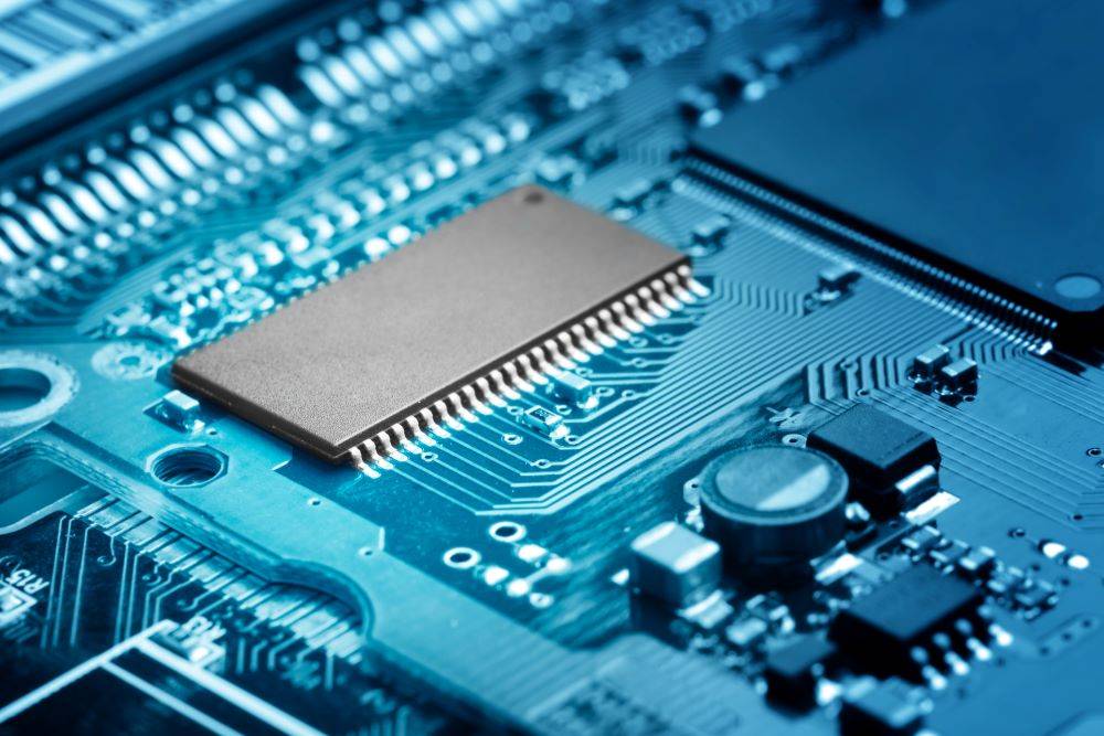
在 半导体芯片领域 在半导体芯片领域,镓(Ga)、铟(In)、砷(As)、碲(Te)和锑(Sb)等高纯度金属发挥着举足轻重的作用。它们的超高纯度对于精确控制导电性和热性能至关重要,而导电性和热性能直接影响半导体器件的性能和可靠性。严格的纯度要求通常需要超过 99.999%,以确保将可能损害集成电路完整性的杂质引起的缺陷降至最低。
光学元件 也从高纯度金属中受益匪浅。例如,铝(Al)和金(Au)等金属可用于制造反射镜、透镜和滤光片。这些金属的高纯度可确保最佳的光透射和反射效果,这对于从高分辨率成像到先进激光系统等各种应用都至关重要。不含杂质可确保光学特性保持不变,从而提供清晰准确的结果。
在 航空航天工业 在航空航天工业中,高纯度金属是制造发动机材料不可或缺的材料。钛(Ti)和镍(Ni)等金属用于涡轮叶片和其他高压力部件。它们在极端温度下的卓越强度、耐腐蚀性和热稳定性对航空航天发动机的耐用性和性能至关重要。这些金属的高纯度可确保它们在高速飞行和重返大气层的恶劣条件下保持机械性能。
此外,高纯度金属还可用于生产 溅射靶材 和 电容器材料 .溅射靶材通常由铜(Cu)和钼(Mo)等金属制成,要求纯度超过 4N5(99.995%),以确保在集成电路中沉积高质量的薄膜。同样,高纯度铝对铝电解电容器也至关重要,纯度必须达到 99.9% 或更高,才能实现所需的电容和可靠性。
高纯度金属还可用于 滤光器 , X 射线探针 以及作为 高性能陶瓷材料的前驱体 .在光学滤光片中,银(Ag)和铬(Cr)等金属的纯度对于实现精确的光谱特性至关重要。在 X 射线探针中,高纯度金属可提供诊断成像所需的灵敏度和分辨率。此外,在陶瓷材料中使用高纯度金属作为前驱体,可确保生产出具有优异机械和热性能的陶瓷。
总之,高纯金属的应用横跨各种尖端技术,每种技术都要求最高的纯度,以确保最佳的性能和可靠性。
高纯金属的制备技术
湿法提纯
湿法纯化方法利用化学反应还原金属离子,并有效地从杂质中分离出来,在制备高纯金属的过程中发挥着关键作用。这些方法对于实现半导体制造和航空航天工程等现代技术应用所需的严格纯度水平是不可或缺的。
湿法净化的主要技术之一是 离子交换 离子交换法是在溶液和固相(通常是树脂)之间进行选择性离子交换。这种方法可以用危害较小或更容易去除的离子取代特定杂质,从而去除这些杂质。该工艺具有高度选择性,可针对特定杂质进行定制,是纯化领域的多功能工具。
溶剂萃取 是另一种关键方法,即使用溶剂从水溶液中选择性地萃取金属离子。这种技术依靠金属离子在不同溶剂中的不同溶解度,实现目标金属与杂质的高效分离。有机溶剂的使用可以提高萃取过程的选择性和效率,对复杂混合物尤其有效。
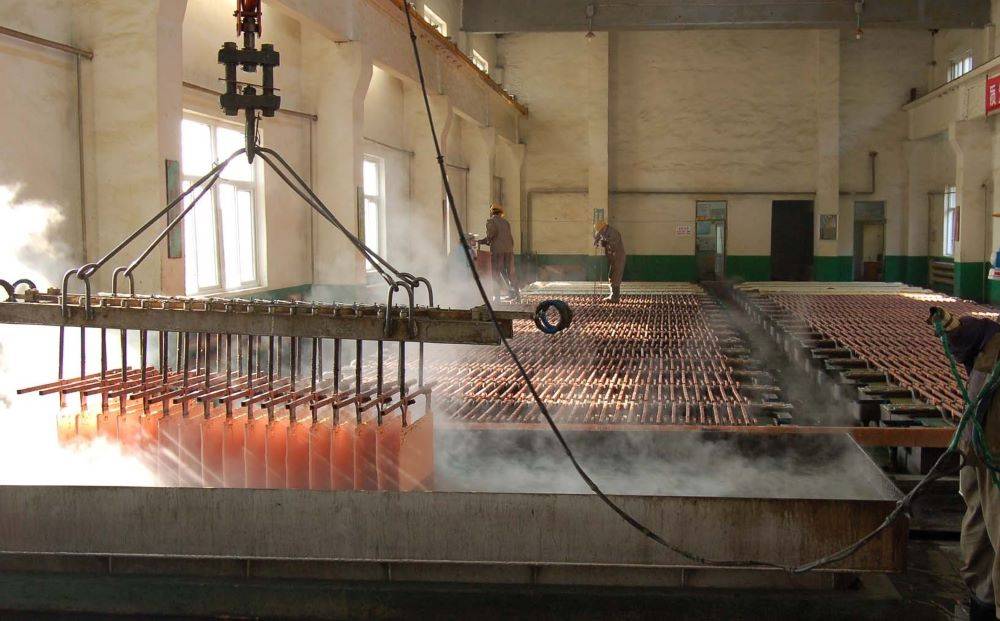
最后、 电解精炼 使用电流将金属从矿石或不纯合金中分离出来。这种方法对导电率高的金属特别有效,因为可以精确控制工艺以达到高纯度水平。电解槽的设计可确保目标金属优先沉积在阴极,而杂质要么留在电解液中,要么作为阳极泥收集起来。
| 方法 | 说明 | 应用实例 |
|---|---|---|
| 离子交换 | 在溶液和树脂之间选择性交换离子 | 稀土金属的提纯 |
| 溶剂萃取 | 使用溶剂从水溶液中选择性地萃取金属离子 | 核工业中铀和钚的分离 |
| 电解提炼 | 利用电流从矿石或不纯合金中分离金属 | 精炼铜和银 |
这些湿法提纯方法不仅对生产高纯度金属至关重要,而且有助于提高金属精炼工艺的整体效率和可持续性。通过采用这些技术,各行业可以实现先进技术所需的高纯度,确保最终产品的卓越性能和可靠性。
火法提纯
火法提纯是生产高纯度金属的关键,它利用高温工艺达到显著的杂质去除水平。这些技术包括真空熔炼、真空蒸馏和等离子弧熔炼,其原理是蒸汽压力差。
在真空熔炼中,金属在真空环境中被加热,使挥发性杂质蒸发并被去除。这种方法对高温下蒸汽压较高的金属特别有效。真空蒸馏则是在真空条件下根据不同的沸点分离成分,确保有选择地去除沸点较低的杂质。
等离子弧熔化是一种更先进的技术,它利用电弧产生高温等离子体,温度可超过 10,000°C 。这种极端高温不仅能熔化金属,还能使杂质气化,然后被等离子体流带走。这种方法对要求超高纯度的金属非常有效。
上述每一种火法提纯方法都在高纯金属的生产中发挥着至关重要的作用,可确保最终产品满足现代技术应用对纯度的严格要求。
高纯金属的应用与发展
半导体材料
镓(Ga)、铟(In)、砷(As)、碲(Te)和锑(Sb)等高纯金属在半导体器件的制造中发挥着至关重要的作用。这些材料是制造晶体管、二极管和集成电路等先进电子元件不可或缺的材料。这些金属的纯度直接影响半导体器件的电气性能和可靠性。
在半导体制造过程中,即使是微量的杂质也会极大地改变材料的电子特性。例如,外来原子的存在会在半导体带隙内产生局部能态,导致不必要的导电性或电荷载流子俘获。因此,这些金属的纯度通常需要超过 99.999% (5N),才能满足半导体行业的严格要求。
高纯金属对半导体性能的影响是多方面的。它们有助于形成高质量的半导体结,这对设备的高效运行至关重要。此外,这些金属还经常用于制造化合物半导体,如砷化镓(GaAs)和磷化铟(InP),与硅基半导体相比,它们具有更优异的电子和光学性能。
此外,高纯度金属在半导体制造中的应用不仅限于其原始形态。它们还被用作掺杂剂,即有意引入的改变半导体导电性的杂质。掺杂剂浓度和分布的精确控制对于在最终设备中实现所需的电气特性至关重要。
总之,高纯金属在半导体技术中的作用怎么强调都不为过。它们卓越的纯度确保了最佳的电气性能、可靠性以及满足现代电子设备日益增长的需求的能力。
溅射靶材
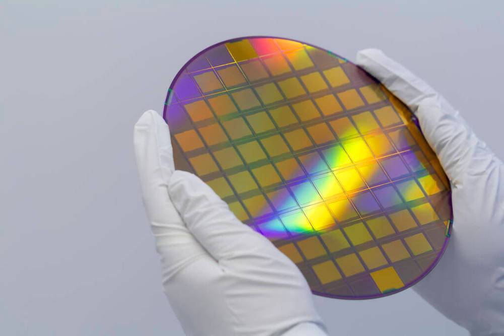
高纯度金属靶材是制造集成电路薄膜不可或缺的材料,其纯度要求通常超过 4N5(99.995%)。这些靶材可以是纯金属、合金,也可以是氧化物或氮化物等化合物,它们都经过精心制作,以确保生产出的薄膜具有最佳性能和可靠性。
KINTEK 是该领域的领先制造商,专门生产高密度、超高纯溅射靶材,纯度从 99.9% 到 99.9999%。这些靶材有多种配置,包括单块或粘结格式,尺寸最大可达 820 毫米。生产过程集成了真空熔融/铸造和热等静压 (HIP) 等先进技术,确保靶材与直流、调频、射频和 HIPIMS/HPPMS 等多种溅射技术兼容。
高纯溅射靶材的重要性怎么强调都不过分。靶材中的任何微量杂质都会导致薄膜缺陷,影响其电气、光学和机械性能。例如,在半导体制造中,即使是微量的杂质也会严重影响设备的性能和可靠性。
为了保证溅射靶材的质量,KINTEK 采用了最先进的分析技术,如 X 射线荧光 (XRF)、辉光放电质谱 (GDMS) 和电感耦合等离子体 (ICP)。这些方法可对目标材料进行全面分析,确保其符合先进应用所需的严格纯度标准。
除标准尺寸外,KINTEK 还提供定制尺寸的靶材和合金成分,以满足特定的研究和工业需求。这种灵活性可确保制造商获得符合其确切规格的溅射靶材,从而进一步提高薄膜沉积工艺的精度和效率。
电容器材料
高纯度铝不仅是铝电解电容器的组成部分,也是其制造的基石。从消费电子产品到工业机械,这些电容器因其电容高、体积小而在各种电子设备中不可或缺。铝的纯度(通常要求不低于 99.9%)确保了电容器的可靠性和使用寿命。
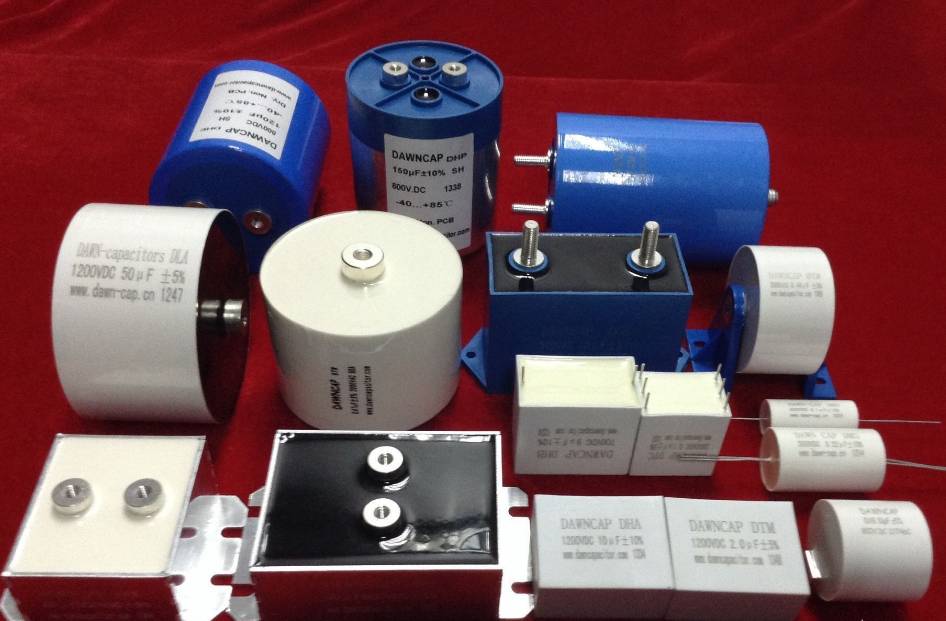
在电容器材料领域,对铝纯度的严格要求是出于对稳定的电气性能和抗腐蚀性的需要。任何微量杂质都可能导致局部腐蚀,进而导致电容器过早失效。因此,选择和制备高纯度铝是生产过程中的关键步骤。
此外,铝的高纯度直接影响电容器有效存储和释放电能的能力。在需要快速传输能量的应用中,如计算机和其他高科技设备的电源中,这种效率是至关重要的。因此,对铝纯度的严格控制可提高最终产品的性能和耐用性。
其他领域
高纯金属在传统领域之外也有广泛的应用,特别是在需要精密可靠材料的先进技术领域。其中一个显著的应用领域是 滤光片 高纯度金属因其卓越的纯度,可用于制造具有高度特定波长选择特性的滤光片。这些滤光片是照相机、望远镜和分光设备等各种光学系统中不可或缺的材料,可提高它们的性能和精确度。
在 医疗诊断领域 在医疗诊断领域,高纯度金属可用于制造 X 射线探针 .这些探针对医学成像技术至关重要,可提供清晰、详细的人体图像。这些金属的纯度确保了最小的背景噪音和最高的清晰度,从而提高了诊断的准确性。
此外,高纯度金属还是 高性能陶瓷材料的前体 .从需要高强度和耐高温的航空航天部件,到需要生物兼容性和耐用性的生物医学植入物,这些陶瓷被广泛应用于各种领域。在生产过程中使用高纯度金属可确保这些陶瓷具有卓越的机械和热性能,满足现代技术的严格要求。
| 应用领域 | 高纯金属的使用 | 优点 |
|---|---|---|
| 光学过滤器 | 用于光学滤波器 | 提高光学系统的性能和精度 |
| X 射线探头 | 用于医学成像 | 通过清晰细致的图像提高诊断准确性 |
| 陶瓷前驱体 | 用作陶瓷前驱体 | 确保高性能陶瓷具有优异的机械和热性能 |