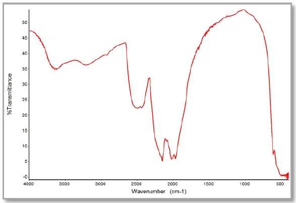
金刚石光学窗口组件概述
金刚石材料简介
金刚石因其在珠宝中的璀璨光芒而闻名于世,同时也是一种具有面心立方结构的第三代超宽带半导体材料。这种独特的结晶形式赋予了钻石一系列非凡的特性,使其非常适合各种先进的技术应用。
金刚石最引人注目的一点是它的机械坚固性。在所有已知材料中,金刚石具有最高的硬度和耐磨性,这确保了它在高压力环境下的耐用性。除机械强度外,金刚石还具有出色的导热性,比铜和银的导热性更强,是需要高效散热的部件的最佳选择。
在光学领域,金刚石的透明度覆盖了从紫外线到红外线的广泛光谱。这种光学多功能性对于高能激光系统、红外传感器甚至 X 射线窗口的应用至关重要。此外,金刚石的电学特性也同样令人印象深刻;它具有高击穿电压和低介电常数的特性,因此非常适合用于大功率电子设备。
这些特性(机械、热、光学和电学)的结合使金刚石成为国防、航空航天和能源领域尖端技术的首选材料。金刚石在极端条件下的可靠性能凸显了其为各行各业带来变革的潜力,使其成为开发新一代光学窗口元件的基石。
金刚石光学元件的合成方法
金刚石光学窗口元件是通过先进的合成技术精心制作而成的,主要采用的方法有 微波等离子体化学气相沉积(MPCVD) , 热丝化学气相沉积 (HWCVD) 和 直流电弧等离子喷射注入化学气相沉积(DCAPCVD)。 .这些技术能够制造出高质量的金刚石薄膜,这对于从辐射传感到高功率激光窗口等各种应用都至关重要。
鉴于所需质与量的天然金刚石的稀缺性和高需求量,大量研究集中于在实验室环境中合成金刚石。值得注意的是,实验室合成金刚石的特性与天然单晶金刚石几乎完全相同,因此是一种可行的替代品。合成方法的选择通常取决于金刚石薄膜的具体应用和所需特性。
例如 化学气相沉积(CVD) 例如,化学气相沉积(CVD)方法尤其适用于生产合成多晶金刚石窗口,这种窗口的形状是直径大、厚度小的圆盘,以最大限度地减少吸收。这些窗口正逐渐取代传统材料,如 硒化锌 等传统材料。此外,最近在 高压高温(HPHT) 和化学气相沉积(CVD)技术的最新进展大大提高了单晶金刚石的纯度和晶体结构,使其适用于大功率辐射源中的衍射光栅和窗口材料等应用。
此外,这些合成方法并不局限于光学应用。它们还可用于制造设计型光学透明金刚石砧,这对于使用金刚石砧单元在超高压下测量材料的电特性和磁特性至关重要。这种多功能性凸显了人造金刚石在当前和新兴技术中的重要性。
金刚石光学窗口元件的应用
红外波段应用
金刚石光学窗口在红外(IR)应用中发挥着关键作用,尤其是在机载、弹道和舰载系统中。这些窗口是红外搜索和跟踪系统不可或缺的组成部分,对于早期探测和跟踪各种军事和监视环境中的目标至关重要。金刚石优异的导热性和透射率使其成为这些应用的理想材料,即使在极端条件下也能确保系统高效运行。
除了用于搜索和跟踪系统,金刚石光学窗口还被用于高能激光武器系统。金刚石光学窗口的高损伤阈值和光学清晰度确保其能够承受激光操作所需的高能量水平,使其成为现代国防技术中不可或缺的材料。
此外,金刚石光学窗口的多功能性还超出了军事应用的范围。它们还可用于民用和商业领域,如先进的成像和光谱系统。金刚石的光谱范围很广,从可见光到远红外,因此成为这些应用的首选,可对各种材料和环境进行精确细致的分析。
| 应用领域 | 金刚石光学视窗的主要优点 |
|---|---|
| 红外搜索和跟踪 | 高热导率,出色的透射率 |
| 高能激光武器 | 损伤阈值高、光学清晰 |
| 先进的成像和光谱分析 | 光谱范围广,分析能力精确 |
金刚石光学窗口的独特性能,如高导热性、光学清晰度和宽光谱范围,使其在各种红外应用中不可或缺,确保了其在军用和民用环境中的卓越性能和可靠性。
微波和太赫兹波段应用
金刚石元件在高功率微波武器和太赫兹行波管的开发中发挥着举足轻重的作用。这些元件因其卓越的透射率和机械强度而不可或缺,这对这些先进系统的性能至关重要。
在微波武器领域,金刚石的高透射率可确保电磁波在传播过程中不会产生明显损耗,从而保持武器的有效性。同样,在太赫兹行波管中,金刚石的机械强度使其能够制造出坚固的部件,以承受与这些设备相关的高压力环境。
此外,金刚石的独特性能使其成为大功率微波和太赫兹应用的理想材料。金刚石能够有效地传输电磁波,同时具有机械耐久性,因此在这些尖端技术中,金刚石是优于其他材料的最佳选择。
| 应用领域 | 金刚石元件的主要优点 |
|---|---|
| 大功率微波武器 | 高透射率、机械强度 |
| 太赫兹行波管 | 高透射率、机械强度 |
在这些应用中集成金刚石元件不仅能提高性能,还为国防和航空航天领域的创新开辟了新的可能性。随着研究和开发的不断深入,金刚石在这些高科技领域的作用预计会越来越大,进一步巩固其作为先进光学窗口元件首选材料的地位。
X 射线和极紫外线应用
金刚石薄膜不仅用于 X 射线窗口,还在极紫外线(EUV)光刻系统中发挥着举足轻重的作用。金刚石薄膜在这些高能光谱中具有超强的透射率,再加上其卓越的机械性能,使其成为先进成像技术中不可或缺的材料。
在 X 射线应用中,金刚石窗口因其在保持高透射率的同时还能承受高压和高温而备受青睐。这使它们成为同步辐射源和 X 射线望远镜的理想选择,因为窗口材料的完整性对准确的数据采集至关重要。
在超紫外线光刻技术中,金刚石薄膜是光学系统的核心部件,对于生产具有纳米级特征的微芯片至关重要。金刚石在超紫外线范围内的高透射率可实现精确成像,而其机械强度则可确保光刻设备的使用寿命和可靠性。
| 应用 | 使用的材料特性 | 主要优点 |
|---|---|---|
| X 射线窗口 | 高透射率、机械强度 | 精确的数据采集、高压下的耐用性 |
| 超紫外线光刻 | 高透射率、机械强度 | 精确成像,设备寿命长 |
金刚石独特的光学和机械特性使其成为这些高要求应用的首选材料,推动了科学研究和工业生产的发展。
金刚石光学元件的制备和加工
曲面加工
开发制备大面积、高质量曲面金刚石薄膜的技术对于需要保形结构的应用至关重要。这些技术对于制造符合复杂几何形状的光学元件至关重要,从而提高其在国防、航空航天和能源等各个领域的性能。
这一领域的主要挑战之一是确保金刚石薄膜在被塑造成曲面时仍能保持其卓越的机械、热和光学特性。这就需要采用先进的加工方法来处理金刚石的独特特性,如硬度和导热性。
| 加工技术 | 主要特点 | 应用 |
|---|---|---|
| 激光切割 | 精确切割,热影响区最小 | 航空航天部件、高精度光学窗口 |
| 离子束加工 | 非接触式高精度表面改性 | 国防光学、保形红外传感器 |
| 化学蚀刻 | 利用化学反应控制材料去除 | 能源行业元件、曲面 X 射线窗口 |
这些技术不仅能制造出曲面金刚石薄膜,还能确保制造出的元件满足先进光学系统对高透光率、机械强度和热稳定性的严格要求。通过掌握这些工艺,研究人员可以突破金刚石光学元件的极限,为高科技应用开辟新的可能性。
表面抛光工艺
实现金刚石光学元件的完美表面抛光是一个复杂的过程,涉及各种先进技术。这些方法大致可分为机械、化学机械、热化学和其他专门工艺,如动态摩擦、激光、离子束、等离子蚀刻和电火花加工 (EDM)。每种技术都有其独特的优势和应用,可满足金刚石光学元件的严格要求。
机械抛光 是最传统的方法之一,依靠研磨材料逐渐去除表面缺陷。这种技术对于在平面上获得光滑的表面特别有效。不过,这种方法耗时较长,而且可能需要多级抛光才能达到理想的光滑度。
化学机械抛光 化学机械抛光将化学反应与机械研磨相结合,可以更精确地控制抛光过程。这种方法尤其适用于传统机械抛光可能会造成损坏的精细表面。
热化学抛光 热化学抛光是利用热量引起化学反应,从而改变钻石表面。这种技术对去除深层缺陷非常有效,并可与其他方法结合使用,以达到极佳的抛光效果。
除了这些主要方法外 专门技术 例如 动态摩擦抛光 , 激光抛光 , 离子束抛光 , 等离子蚀刻 和 电火花加工 提供了独特的功能。例如,动态摩擦抛光利用高速旋转和摩擦来平滑表面,而激光抛光则利用激光束以高度可控的方式去除材料。离子束抛光使用加速离子来蚀刻表面,提供非常精细和可控的抛光效果。等离子体蚀刻则使用等离子体去除材料,精度极高。最后,电火花加工(EDM)或放电加工使用放电来侵蚀材料,是复杂形状和难以触及区域的理想加工方法。
这些方法中的每一种都在金刚石光学元件的制造过程中发挥着至关重要的作用,可确保其达到在国防、航空航天和能源等各个领域的预期应用所需的高标准。
结论和未来方向
金刚石光学窗口优势概述
金刚石光学窗口元件利用金刚石的优异特性,在众多高科技应用领域,特别是国防和能源领域,发挥着卓越的作用。金刚石具有无与伦比的硬度、化学惰性、高热导率和低热膨胀系数,使其成为传输红外线和微波辐射的最佳选择。这种优越性体现在它越来越多地被用作高功率 CO2 激光器和陀螺仪的输出窗口,取代了传统材料,如 硒化锌 .
通过化学气相沉积(CVD)技术生产的合成多晶金刚石窗口被塑造成大直径、最小厚度的圆盘,以减少吸收,使其成为高功率应用的理想选择。此外,尺寸高达约 10 毫米的单晶金刚石板块在各种光学领域中正变得举足轻重,包括激光腔内的散热器、衍射光学以及拉曼激光器中的增益介质。
高压高温(HPHT)和化学气相沉积(CVD)合成技术的最新进展大大提高了单晶金刚石的纯度和晶体学完美性,使其能够用作同步加速器等高功率辐射源的衍射光栅和窗口材料。CVD 和 HPHT 工艺还可用于制造光学透明的金刚石砧,这是使用金刚石砧测量超高压下材料的电特性和磁特性的重要工具。
CVD 金刚石的光学应用大致分为自支撑薄膜窗口、光学晶体和光学涂层。这些应用横跨从 X 射线到微波的所有波段,使金刚石窗口成为微波系统、导弹窗口/护舷、X 射线窗口、激光窗口、微透镜以及核聚变、机载、弹载、舰载和天基系统中其他组件不可或缺的组成部分。
如表 3 所示,金刚石的独特特性,如原子密度高、结合力强,再加上高度对称的晶格结构,使其具有显著的拉曼增益。此外,如表 4 所示,其高折射率和声波传输速度也有助于产生高布里渊增益和频移。这些特性使金刚石晶体成为高功率、高效率拉曼和布里渊激光操作的理想介质。
总之,金刚石光学窗口因其卓越的性能,正在彻底改变高科技应用,使其成为国防、能源和其他众多领域不可或缺的材料。
挑战与研究需求
对大尺寸光学级金刚石制备和精密加工的需求仍然是一项重大挑战,尤其是在高功率、高温和高频率应用领域。这些应用不仅需要合成大型无瑕金刚石,还需要对其进行精确成型和抛光,以满足对光学清晰度和机械强度的严格要求。
目前,制备金刚石光学元件的方法有 微波等离子体化学气相沉积法 和热丝化学气相沉积等制备金刚石光学元件的方法在放大生产大尺寸金刚石方面受到限制。此外,表面抛光工艺(包括机械、化学机械和激光抛光等技术)也必须加以改进,以确保金刚石表面不存在可能影响其光学性能的缺陷。
此外,在某些应用(如曲面加工)中对保形结构的需求也增加了复杂性。开发能够高效生产大面积、高质量曲面金刚石薄膜的技术至关重要,但这一领域仍需取得重大进展。
总之,虽然金刚石光学窗口元件在各种高科技领域具有无与伦比的优势,但其制备和加工工艺必须进行重大改进,才能完全满足现代应用的需求。
相关产品
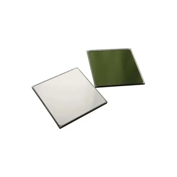
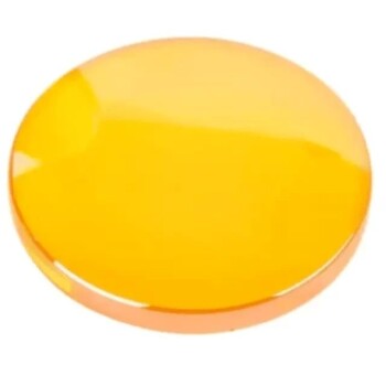
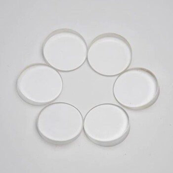
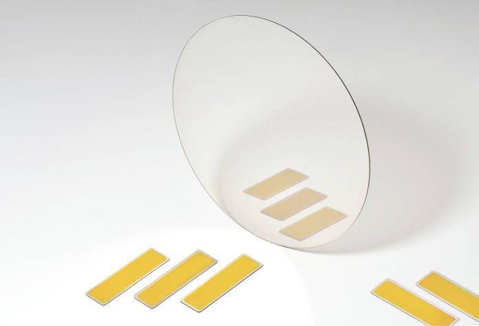
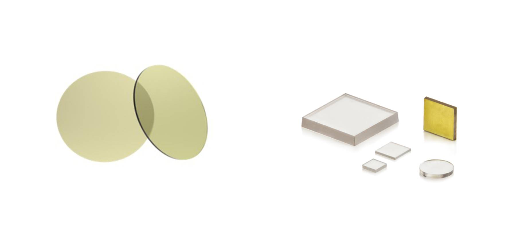
- 实验室应用的CVD金刚石光学窗口
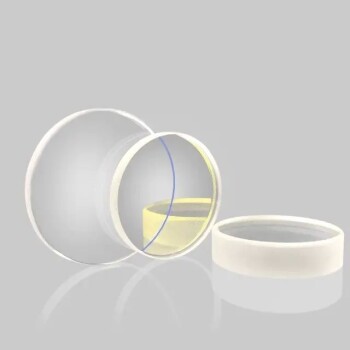
- 用于光学应用的MgF2氟化镁晶体衬底窗口
- 光学窗口玻璃基板晶圆石英片 JGS1 JGS2 JGS3
- 光学窗口玻璃基板晶圆单双面镀膜K9石英片
- 红外透射涂层蓝宝石片基板窗口