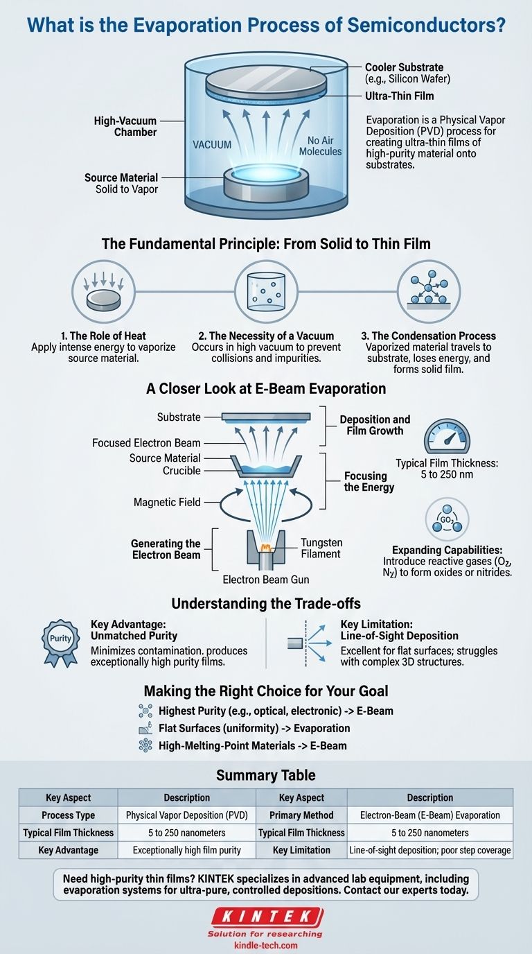
知识 半导体的蒸发过程是怎样的?
作者头像

技术团队 · Kintek Solution

更新于 1周前

半导体的蒸发过程是怎样的?

The evaporation process of semiconductors involves the use of techniques such as thermal evaporation and e-beam evaporation to deposit thin films of materials onto substrates. These processes are part of Physical Vapor Deposition (PVD) and are crucial in the semiconductor industry for the manufacturing of integrated circuits and microprocessors.

Thermal Evaporation: Thermal evaporation involves heating a material using a resistive heat source until it reaches its vapor pressure. The vapor then condenses on a substrate, forming a thin film. This method is versatile and can deposit a wide range of materials, including metals and semiconductors. The thickness of the film can be controlled by adjusting parameters such as the temperature of the evaporant, the rate of deposition, and the distance between the evaporant and the substrate. Thermal evaporation is commonly used in the production of electronic and optical devices like solar cells and OLED displays.

E-beam Evaporation: E-beam evaporation uses a highly-charged electron beam to heat and evaporate the source material. The intense heat from the electron beam melts the material, causing it to evaporate. The evaporated particles then flow in a vacuum chamber towards the substrate, forming a thin, high-purity coating. This process is particularly useful for depositing materials that require high purity and precise control of thickness, often used in optical thin films such as those found in glasses and solar panels.

Applications and Challenges: In the semiconductor industry, these evaporation techniques are used for depositing metal and metal oxide films onto silicon wafers. These films are critical components in the manufacturing of integrated circuits and microprocessors. However, challenges such as non-uniform deposition due to substrate roughness (shadowing effect) and reactions with foreign particles in the environment can affect the quality and uniformity of the deposited films. Additionally, performing evaporation in poor vacuum conditions can lead to non-uniform and discontinuous films.

Conclusion: The evaporation process in semiconductors is a critical step in the fabrication of thin films used in various electronic and optical devices. Both thermal and e-beam evaporation techniques offer unique advantages and are tailored to specific requirements of material purity and film thickness control, essential for the high-performance demands of modern semiconductor devices.

Discover the precision and purity that KINTEK SOLUTION brings to your semiconductor evaporation needs. Our cutting-edge thermal evaporation and e-beam evaporation systems are designed to meet the exacting demands of integrated circuit and microprocessor production. Trust our advanced PVD solutions to control film thickness with precision, ensuring high-purity coatings for solar cells, OLED displays, and more. Elevate your semiconductor fabrication with KINTEK SOLUTION—where quality and consistency are our core values. Contact us today and take your thin-film deposition to the next level.

相关产品

等离子体增强蒸发沉积 PECVD 涂层机

等离子体增强蒸发沉积 PECVD 涂层机

使用 PECVD 涂层设备升级您的涂层工艺。是 LED、功率半导体、MEMS 等领域的理想之选。在低温下沉积高质量的固体薄膜。

电子束蒸发石墨坩埚

电子束蒸发石墨坩埚

主要用于电力电子领域的一种技术。它是利用电子束技术,通过材料沉积将碳源材料制成的石墨薄膜。

电子枪光束坩埚

电子枪光束坩埚

在电子枪光束蒸发中,坩埚是一种容器或源支架,用于盛放和蒸发要沉积到基底上的材料。

电子束蒸发涂层无氧铜坩埚

电子束蒸发涂层无氧铜坩埚

电子束蒸发涂层无氧铜坩埚可实现各种材料的精确共沉积。其可控温度和水冷设计可确保纯净高效的薄膜沉积。

有机物蒸发舟

有机物蒸发舟

有机物蒸发舟是在有机材料沉积过程中实现精确均匀加热的重要工具。

有机物质的蒸发坩埚

有机物质的蒸发坩埚

有机物蒸发坩埚,简称蒸发坩埚,是一种在实验室环境中蒸发有机溶剂的容器。

石墨蒸发坩埚

石墨蒸发坩埚

用于高温应用的容器,可将材料保持在极高温度下蒸发,从而在基底上沉积薄膜。

电子束蒸发涂层钨坩埚/钼坩埚

电子束蒸发涂层钨坩埚/钼坩埚

钨和钼坩埚具有优异的热性能和机械性能,常用于电子束蒸发工艺。

射频等离子体增强化学气相沉积系统 射频等离子体增强化学气相沉积系统

射频等离子体增强化学气相沉积系统 射频等离子体增强化学气相沉积系统

RF-PECVD 是 "射频等离子体增强化学气相沉积 "的缩写。它能在锗和硅基底上沉积 DLC(类金刚石碳膜)。其波长范围为 3-12um 红外线。

钼/钨/钽蒸发舟

钼/钨/钽蒸发舟

蒸发舟源用于热蒸发系统,适用于沉积各种金属、合金和材料。蒸发舟源有不同厚度的钨、钽和钼,以确保与各种电源兼容。作为一种容器,它可用于材料的真空蒸发。它们可用于各种材料的薄膜沉积,或设计成与电子束制造等技术兼容。

镀铝陶瓷蒸发舟

镀铝陶瓷蒸发舟

用于沉积薄膜的容器;具有铝涂层陶瓷本体,可提高热效率和耐化学性。

陶瓷蒸发舟套装

陶瓷蒸发舟套装

它可用于各种金属和合金的气相沉积。大多数金属都能完全蒸发而不损失。蒸发筐可重复使用1。

电子束蒸发涂层导电氮化硼坩埚(BN 坩埚)

电子束蒸发涂层导电氮化硼坩埚(BN 坩埚)

用于电子束蒸发涂层的高纯度、光滑的导电氮化硼坩埚,具有高温和热循环性能。


留下您的留言