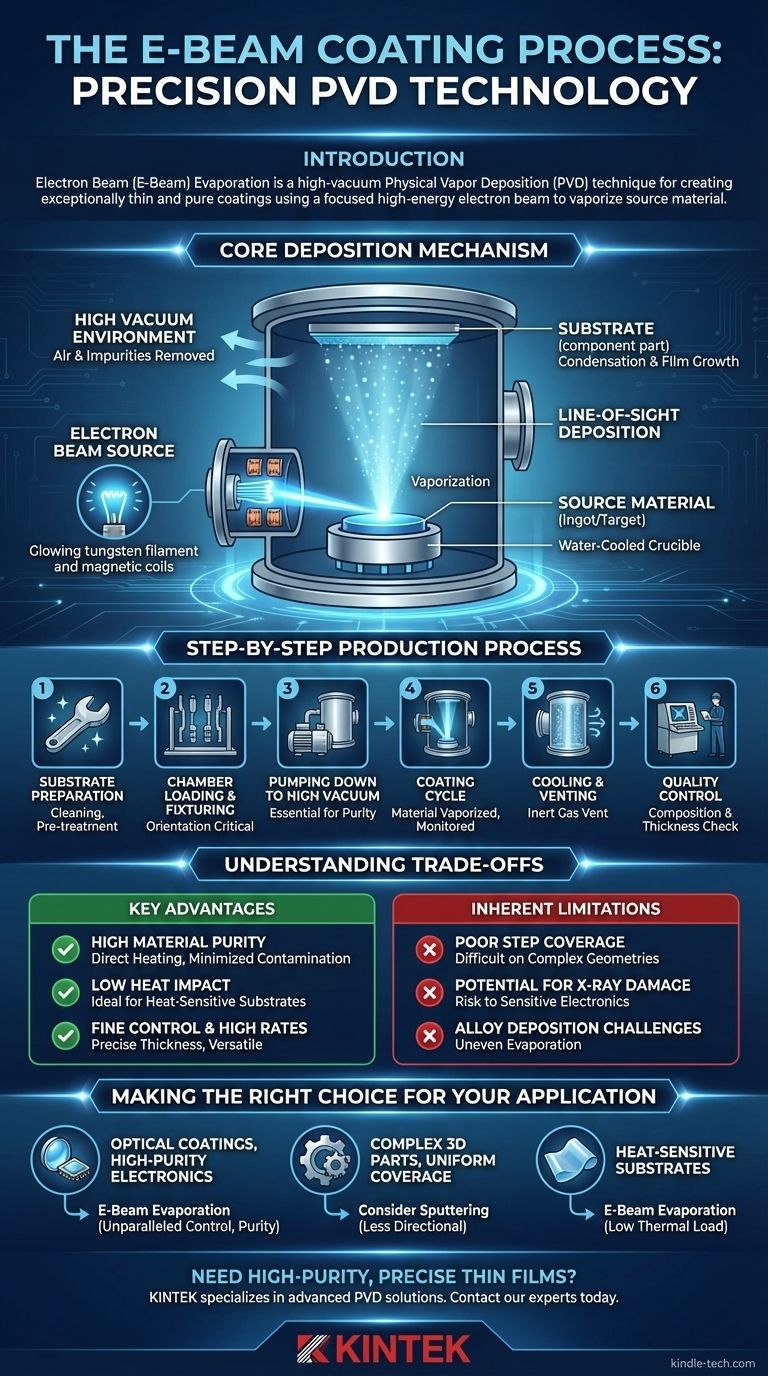
电子束 (E-Beam) 蒸发是一种高真空物理气相沉积 (PVD) 技术,用于制造极其薄且纯净的涂层。该过程使用聚焦的高能电子束加热源材料,使其汽化。然后,该蒸汽沿直线传播并冷凝到基板上,形成精确的、逐原子堆积的薄膜。
电子束镀膜本质上是一种视线 (line-of-sight) 沉积过程,因其精度和对被涂覆部件的热影响小而备受推崇。它擅长制造用于专业应用的超纯、致密薄膜,但其定向特性对复杂三维几何形状的涂覆带来了挑战。
核心沉积机制
要理解电子束过程,必须掌握真空室内发生的物理学原理。每个步骤都经过精确控制,以实现特定的薄膜成分和厚度。
真空环境
整个过程在高真空室内进行。抽空腔室对于去除空气和其他气态杂质至关重要,这些杂质可能会与汽化材料发生反应并污染最终薄膜。这种近乎真空的状态还允许蒸汽原子直接传输到基板,而不会与其他粒子碰撞。
电子束源
加热钨丝以产生电子流。然后使用一系列磁场加速并将这些电子聚焦成高能光束,这类似于阴极射线管 (CRT) 电视的工作方式。
汽化源材料
这个聚焦的电子束被导向源材料(通常称为锭或靶材),它被放置在一个水冷铜坩埚中。光束的强烈能量将材料加热到其沸点,使其蒸发或升华成蒸汽。
视线沉积
蒸汽原子从源头沿直线、直接的路径传输到基板。这种“视线”特性意味着涂层仅沉积在可从蒸发源直接看到的表面上。
冷凝与薄膜生长
当蒸汽原子到达相对较冷的基板表面时,它们会冷凝。这个过程逐层、逐原子地构建涂层,形成非常细晶粒和致密的薄膜。
分步生产过程
从核心机制过渡到工业应用涉及一系列精心管理的生产步骤。
第 1 步:基板准备
没有原始表面,就不可能实现适当的附着力。此步骤涉及严格清洁以去除任何污染物。根据部件的历史,它可能还包括剥离旧涂层或进行特定的预处理以准备表面。
第 2 步:腔室装载与夹具安装
源材料放置在坩埚中,基板安装在专用夹具或支架上。由于过程的视线特性,这些夹具的定位至关重要,以确保目标表面正确暴露于蒸汽流中。
第 3 步:抽真空至高真空
装载后,腔室被密封并抽真空至目标压力水平。这个抽真空过程可能需要相当长的时间,但对于最终涂层的纯度至关重要。
第 4 步:涂层循环
建立真空后,激活电子束并汽化材料。实时监测沉积速率和最终厚度,以确保薄膜满足精确的规格。整个循环可能从三十分钟到几小时不等,具体取决于材料和所需的厚度。
第 5 步:冷却与排气
达到目标厚度后,电子束停止工作。系统冷却,然后用惰性气体对腔室进行排气,使其恢复到大气压。
第 6 步:质量控制
每个批次都要经过严格检查。技术人员使用X射线荧光 (XRF) 等工具来验证涂层的成分和厚度,确保其符合所有要求的标准。
理解权衡
没有一种涂层技术对所有应用都是完美的。电子束蒸发具有明显的优点和局限性,这些决定了其理想的应用场景。
主要优点
- 高材料纯度: 电子束仅直接加热源材料,而不是整个坩埚,从而最大限度地减少污染,并形成极其纯净的薄膜。
- 低热影响: 与其他方法相比,该过程对基板的热量传递较少,因此非常适合涂覆热敏材料,如塑料、聚合物或预组装的电子元件。
- 精细控制和高速率: 它允许对沉积速率和薄膜厚度进行非常精确的控制,同时还能够以很高的蒸发速率处理各种材料,包括金属和陶瓷。
固有局限性
- 步进覆盖率差: 高度定向的蒸汽流使得难以均匀涂覆复杂形状、尖锐边缘或内部表面。它主要涂覆其能“看到”的部分。
- 潜在的 X 射线损伤: 高能电子与源材料的相互作用会产生 X 射线。虽然通常水平较低,但这些射线可能足以损坏高度敏感的电子基板或光学元件。
- 合金沉积挑战: 蒸发由具有不同蒸汽压力的多种元素(合金)组成的材料可能很困难,因为挥发性较高的元素会首先蒸发。
为您的应用做出正确的选择
选择正确的 PVD 方法需要将工艺能力与您的主要工程目标相匹配。
- 如果您的主要重点是光学涂层或高纯度电子产品: 电子束蒸发在薄膜厚度、纯度和密度方面提供了无与伦比的控制,这对这些应用至关重要。
- 如果您的主要重点是复杂 3D 零件的均匀覆盖涂层: 您应该考虑溅射等定向性较差的 PVD 方法,以确保所有表面都得到充分涂覆。
- 如果您的主要重点是热敏基板的涂覆: 电子束工艺的低热负荷使其成为保护聚合物或精致预组装元件等材料的优选方法。
最终,选择电子束蒸发是一项战略决策,适用于最终薄膜质量和精度比均匀几何覆盖更重要的应用。
摘要表:
| 关键方面 | 详细信息 |
|---|---|
| 工艺类型 | 物理气相沉积 (PVD) |
| 环境 | 高真空 |
| 机制 | 视线沉积 |
| 主要优点 | 高纯度、低热影响、精确的厚度控制 |
| 理想用途 | 光学涂层、高纯度电子产品、热敏基板 |
| 局限性 | 复杂 3D 几何形状的覆盖率差 |
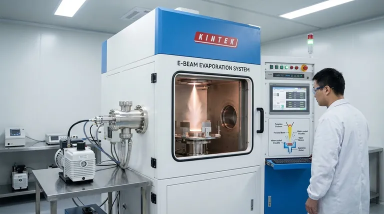
需要为您的研究或生产提供高纯度、精确的薄膜吗?
KINTEK 专注于先进的实验室设备,包括用于苛刻应用 (demanding applications) 的 PVD 解决方案。我们的专业知识可以帮助您选择正确的涂层技术,以确保您的特定基板和目标获得卓越的薄膜质量、纯度和性能。
立即联系我们的专家,讨论我们如何支持您实验室的薄膜沉积需求。
图解指南