当我们谈论薄膜的“范围”时,我们指的不是单一的指标,而是这项技术在四个关键维度上的广阔范围。其物理厚度通常从几纳米到几微米不等。更重要的是,其范围涵盖了极其多样的材料、广泛的功能特性谱系,以及不断扩大的高科技应用列表,从微芯片到医疗设备。
薄膜技术的核心概念不只是其物理尺寸,而是它作为一个多功能平台的作用。通过在纳米尺度上精确控制材料层,我们可以设计出在块体材料中无法实现的独特光学、电学和机械性能。
界定“范围”:薄膜厚度
对“范围”最字面的解释是厚度。这个维度是所有其他特性的基础。
从单个原子到微米
薄膜是材料的一层,其厚度可以从单个原子层(分数纳米)到几微米(µm)不等。
大多数工业应用的工作范围在 10 纳米到 10 微米之间。这个尺度是材料薄到足以表现出独特性能,同时又足够厚以保持稳固和功能性的最佳点。
为什么厚度很重要
在这些微小尺寸下,在块体材料中可忽略的效应会变得占主导地位。这包括量子力学现象、光学干涉和独特的应力-应变关系,使得工程师可以通过简单地调整厚度来微调材料的性能。
材料和工艺的范围
薄膜技术的多功能性直接与其可以沉积的材料种类和实现沉积方法的精度相关联。
从金属到先进陶瓷
几乎任何类别的材料都可以制成薄膜。参考资料中提到了广泛的选择,包括:
- 金属:铝、难熔金属
- 电介质和陶瓷:氧化硅、氮化物 (TiN)
- 半导体:硅、锗、化合物半导体 (GaAs)
- 特种材料:类金刚石碳 (DLC) 和新兴的无定形氧化物
这种材料的多样性使得可以为几乎任何工程挑战量身定制涂层。
实现精度的工艺
制造这些薄膜需要在高度受控的环境和复杂的设备下进行。关键方法包括:
- 化学气相沉积 (CVD):使用前驱体气体在表面上“生长”薄膜,非常适合制造均匀、高纯度的层。
- 物理气相沉积 (PVD):涉及在真空中汽化固体材料(溅射或蒸发)并使其在基底上凝结,非常适合金属和硬质涂层。
- 离子注入:将带电原子(离子)注入表面以改变其化学和物理特性。
可实现性能的光谱
将材料沉积为薄膜是为了实现与块体材料不同的特定功能特性。
控制光学特性
薄膜在控制光方面至关重要。它们可以被设计成对显示器高度透明,对镜片具有抗反射性,或对镜子具有高反射性。
控制电学行为
薄膜的电学特性可以被精确调整。它们可以充当微芯片布线中的导体、电容器中的绝缘体(电介质)或晶体管中的半导体。
增强机械耐久性
薄膜通常用作保护涂层。氮化钛 (TiN) 和类金刚石碳 (DLC) 等材料为切削工具和耐磨部件创造了超硬、抗刮擦和低摩擦的表面。
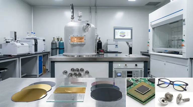
现代应用的广度
材料和性能的结合使薄膜具有极其广泛的应用,这些应用定义了现代技术。
- 半导体制造:构成每个集成电路的基础,在硅片上创建晶体管、导线和绝缘体。
- 显示器和光学:支持从平板电视和智能手机屏幕到镀膜眼镜和高性能镜片的一切。
- 数据存储:用于创建硬盘中的磁性层和光盘中的相变层。
- 医疗设备:为植入物提供生物相容性涂层,为手术工具提供耐用、无菌的表面。
理解固有的权衡
尽管功能强大,薄膜技术并非没有挑战和局限性。理解这些是成功应用的关键。
成本和复杂性
用于 CVD 和 PVD 等沉积过程的设备价格昂贵,并且操作和维护需要专业知识。这为制造设置了很高的进入门槛。
基底依赖性
薄膜必须沉积在基底(如硅片或玻璃片)上。薄膜的附着力、应力和最终性能在很大程度上取决于该基底的选择及其表面处理。
耐用性和稳定性
极薄的层可能很脆弱,容易受到划伤、分层或环境降解。实现所需特性(如透明度)通常需要以牺牲长期耐用性为代价。
如何根据您的目标来界定“范围”
理解薄膜技术的“范围”的最佳方式是通过您特定目标的视角。
- 如果您的主要关注点是材料科学或研发: 新材料组合的范围,例如用于透明晶体管的无定形氧化物,是最关键的创新领域。
- 如果您的主要关注点是制造和工程: 沉积工艺(CVD、PVD)的范围以及您控制它们以实现一致薄膜性能的能力是您的关键变量。
- 如果您的主要关注点是产品开发: 应用的范围,从光学到电子及其他领域,定义了该技术可以提供竞争优势的市场机会。
归根结底,薄膜是一项基础技术,使我们能够在微观尺度上设计物质。
摘要表:
| 范围方面 | 关键细节 |
|---|---|
| 厚度 | 单个原子(<1 nm)到几微米(µm) |
| 材料 | 金属 (Al, Ti)、陶瓷 (TiN)、半导体 (Si, GaAs)、DLC |
| 关键特性 | 光学(透明度)、电学(导电性)、机械(硬度) |
| 主要应用 | 半导体、显示器、数据存储、医疗设备 |
准备好利用精密薄膜来设计卓越的表面了吗? KINTEK 专注于用于薄膜沉积(CVD、PVD)和分析的先进实验室设备和耗材。无论您从事研发还是制造,我们的解决方案都能帮助您实现一致、高性能的涂层。请立即联系我们的专家,讨论我们如何支持您的特定实验室需求并加速您的创新。
图解指南


